Research Topics
微波介電質之研發及高頻元件應用
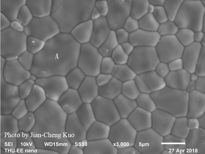
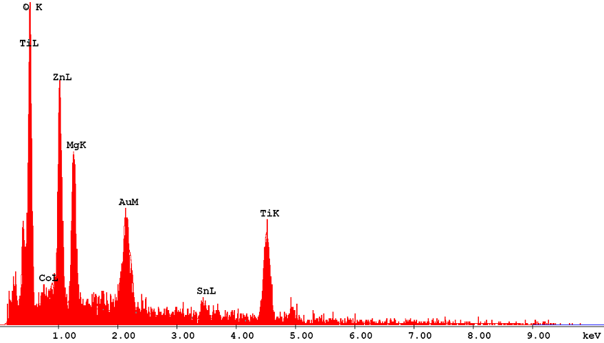
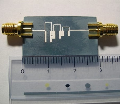
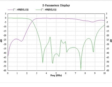
Due to the rapid development of mobile communication, mobile telephone systems, and satellite broadcasting systems, the design of high-quality electronic devices is very important. To satisfy this demand, a material should have a reasonably high dielectric constant (εr > 20) to allow size reduction of the component, a low dielectric loss (Q > 5000, where Q= 1/tan ı) in the microwave frequency range, and temperature stability (𝜏f = 0). Small temperature coefficients of resonant frequency ensure the stability of microwave components at different working temperatures. For microwave circuit designs, each dielectric property needs to be precisely controlled. Using two or more compounds with negative and positive temperature coefficients to form a solid solution or mixed phases isthe most promising method of obtaining a zero temperature coefficientof resonant frequency, as reported in our previous reports.
半導體元件設計及製程技術
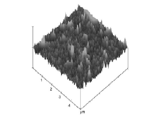
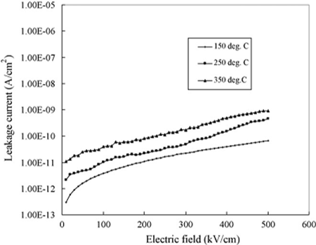
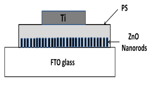
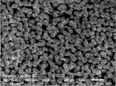
In recent years, several new memory technologies have been developed to address the downscaling issue in conventional random access memory. Among them, resistive switching randomaccessmemory (RRAM) is seen as themost promising technology for futurememory applications. Its simple metal-insulator-metal (MIM) structure makes RRAM easy to fabricate and highly scalable. ZnO nanostructures into organic/polymer layers have been proposed as insulator layers for the MIM structure of RRAM devices because nanostructures can improve the conductivity. Owing to wide direct band gap of and large exciton binding energy at room temperature, ZnO nanorods are application for optoelectronic and semiconductor devices. On the other hand, the potential radiation hardness of RRAM devices has also attracted attention for aerospace and nuclear plant applications
第三類半導體薄膜沉積及元件應用
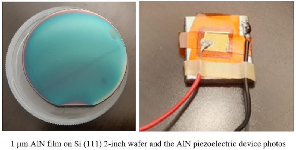
The 3rd generation semiconductors are those materials with a wide bandgap (Eg ~3 eV or above), represented by silicon carbide (SiC) and gallium nitride (GaN). AlN as the material in nitride family, with an ultrawide bandgap of ~6 eV, large piezoelectric coefficient (d33 > 5 pmV-1), nontoxicity, and high surface acoustic wave (SAW) velocity (6105 cm/s) offers tremendous potential for many crucial technologies including electric vehicles (high power), beyond 5G communication (high frequency, acoustic), energy harvesters/sensors (piezoelectric), pandemic prevention (UVC photonics), quantum computing (quantum photonics). Recently, the formation of AlN thin film/structure on Si is attracted great attention and such device applications are being intensively studied due to the low cost of the large size commercial available Si substrates and the potential to integrate with CMOS ICs. Such AlN-on-Si technology makes it possible to integrate both nitride and silicon technologies and could be adapted into mass production rapidly. To meet the needs of the AlN-on-Si technology and the requirement of AlN-based devices fabrication, a high-quality AlN epitaxial layer is necessary. Our approach is to optimize the sputtering conditions of AlN thin film deposited on Si substrate, design and fabricate the novel devices for their unique material properties applications.
紅外線及紫外線感測器與應用
Ever since the first observation of the intersubband transition of GaAs/AlGaAs quantum wells, infrared detectors based on this structure have received much interest over the past decades. Due to the mature growth and processing technology, the large scale focal plane array based on quantum well infrared photodetectors (QWIPs) has been demonstrated with high performance.1–8 Among them, the superlattice (SL) is another promising structure for infrared detection. Generally, the structure of superlattice infrared photodetectors (SLIPs) consists of a SL and a single barrier whose functions are not only to reduce the dark current but also to act as a bias-tuned energy filter.9 Because the applied bias is only dropped on the single barrier, the lower bias is needed for SLIP operation and is good for low dark current and low power consumption.

Oxide material, such as Ga2O3 has attracted significant attention due to its wide bandgap and excellent properties for transparent electronics, solar-blind photodetectors, and next-generation power devices. To adapt the β-Ga2O3-based photodetector to an even shorter response wavelength in the deep UV range, we applied a simple and easy-to-control Thermal Interdiffusion Alloying (TIA) method to fulfill bandgap tunning requirements. With such a unique technique, the β-(AlGa)2O3 films with both Al% content controllable and good crystal quality were demonstrated, which is superior to the other direct-deposition methods. The method we applied here is promising to obtain bandgap tunable β-(AlGa)2O3 thin-film for deep-UV photodetector application by simply using a single Ga2O3 target.

智慧聯網系統設計及實現
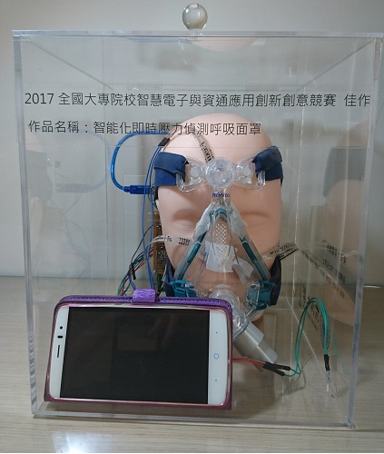
In normal cases, nursing people can only apply force with a texture strength, because the pressure may be too large (greater than 32 mmHg (2.25psi) and the time of 2 hours or more) and cause early bedsores. Pressure sores are recently very common in the health care. According to statistics, pressure sores prevalence in long-term care facility was 1.9-23.9% (Thomas, 2003), in home care agencies to 0% -17.0% (Lyder, 2008). Pressure sores are therefore urgently needed to be issues of concern.
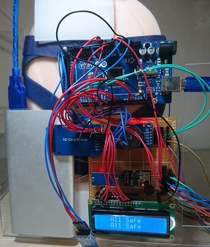
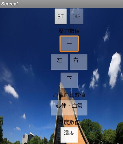
In this study, thin-film pressure sensor with ultra-thin thickness and ultra-low sensing area was embedded into a breathing mask. The thin-film pressure is made of polyster which is the same materials as clothing and towel and therefore suit for long time touched by skin. We also choose same color (as breathing mask) signal transmission line and connected to an external display screen, which is designed with the time when the pressure points to the skin may be hazardous to patients or signal occurs when the alarm sounds, the last and this coupled with wireless transmission module control computer warning signals transmitted to face pressure to monitor patients' conditions, to provide faster and immediate monitoring.
In this study, thin-film pressure sensor with ultra-thin thickness and ultra-low sensing area was embedded into a breathing mask. The thin-film pressure is made of polyster which is the same materials as clothing and towel and therefore suit for long time touched by skin. We also choose same color (as breathing mask) signal transmission line and connected to an external display screen, which is designed with the time when the pressure points to the skin may be hazardous to patients or signal occurs when the alarm sounds, the last and this coupled with wireless transmission module control computer warning signals transmitted to face pressure to monitor patients' conditions, to provide faster and immediate monitoring.
